
A board that works, and files your fab can build without questions.
We take your product from requirements to a routed, manufacturable board: the schematic, the layout, and a bill of materials made of parts you can actually buy.
Clayton, North Carolina. Serving Raleigh and the Triangle. Ships nationwide.
You have a product to build and no one in-house to design the board.
Maybe it is a first prototype, or a product that has outgrown a hand-wired proof of concept, or a board your last designer left without documentation. Either way you need a design you can read a year from now, parts you can order, and a file package a fab and an assembler accept the first time.
Everything needed to order the board.
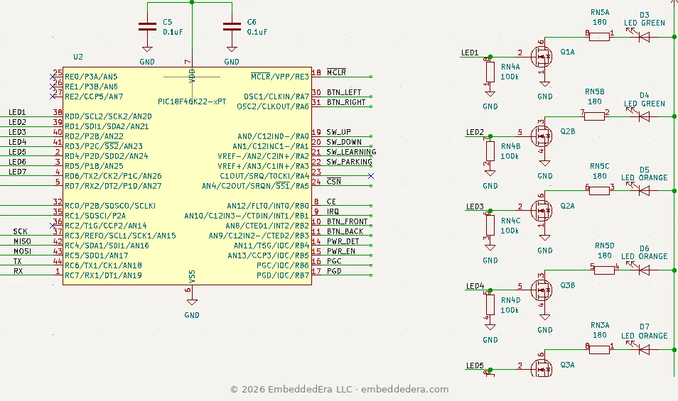
- Schematic A clean, reviewable schematic as PDF plus KiCad source, with design notes on any non-obvious part choice.
- Board layout A routed board in KiCad, impedance-controlled where the signal needs it, laid out against the parts it actually places.
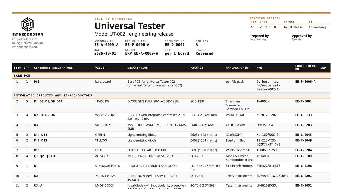
- Bill of materials with alternates Sourceable parts with sourcing notes and alternates called out per line, checked before anything is ordered.
- Fab and assembly outputs Gerbers, drill files, pick-and-place files, fabrication drawing, and stack-up notes.
- Design review A DFM review of footprints, orientation and panelization, treated as a manufacturing decision rather than fixed after the fact.
Four steps from idea to release package.
- 01 Tell us what it has to do Send the product description, interfaces, rough board size, expected quantity and any existing files through the quote form.
- 02 Schematic We draw the schematic and choose the key parts with you.
- 03 Layout and BOM We place and route the board, build the bill of materials with alternates, and run a DFM review.
- 04 Release package You receive the fab and assembly outputs and the files listed in your quote, checked before they go out.
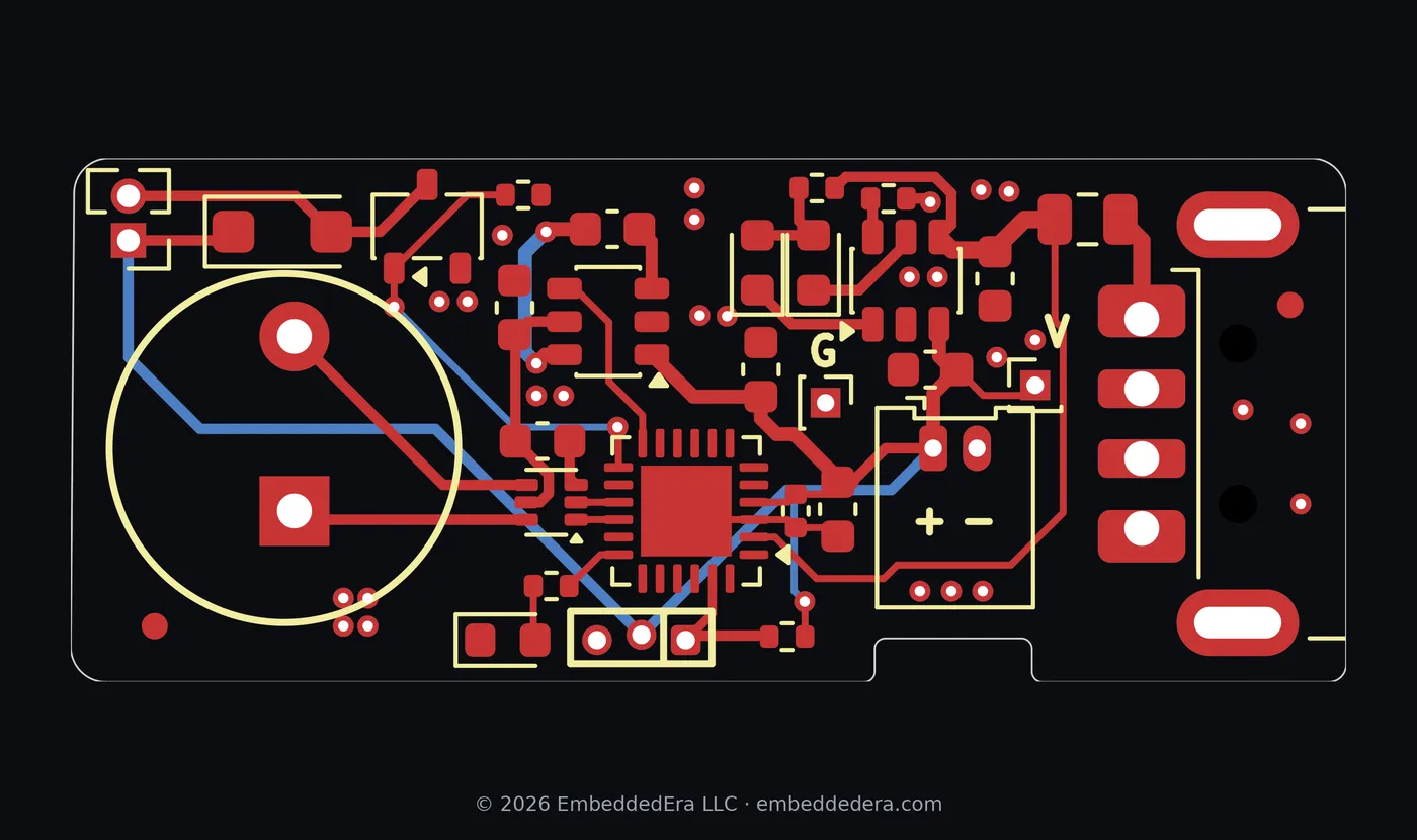
Our own boards, schematics and BOMs.
These are our own design files, not renderings from a stock library.
Before you ask
What do I receive at the end of a PCB design job?
You receive the schematic (PDF + KiCad source), routed board files (KiCad), bill of materials, Gerbers, drill files, pick-and-place files, fabrication drawing, and stack-up notes. The bill of materials carries sourcing notes and alternates.
Do you design in KiCad, and what files do I receive?
Yes, we lay out in KiCad. The deliverables for your project are listed in your quote.
What should I send to get a PCB design quote?
A short description of what the product does, its interfaces, the approximate board size, the quantity you expect, any special requirements and any existing files. The PCB design request in the quote form asks for exactly these.
Notes and tools that go with this.
Tell us about your board.
All servicesClayton, North Carolina. Serving Raleigh and the Triangle. Ships nationwide.